Intel Says 14A Defects Are Falling Fast. It Hasn't Published a Single Number.

- The claim is a comparison between two numbers Intel has not published. David Zinsner said 14A is ’tracking better than the target curve we had for 14A’ — the defect density is not public and neither is the target curve, so the statement cannot be checked from outside.
- There is a precedent and it belongs to Intel. Two years ago the company put a hard defect-density figure for 18A on its own newsroom, over a named executive’s byline, and leaned on it to justify dropping a node. Nothing of that shape has been published for 14A, which is what makes the silence worth noticing rather than routine.
- ‘We have not seen this performance since 22nm’ is a claim about the rate of decline, not the level. It is also, read literally, a statement that every Intel node between 22nm and 14A brought defects down more slowly than this one.
- Defect density is not yield, and the gap between them is die size. Run the standard model at one defect density and a 110 mm² phone die comes out at 90% while a 600 mm² accelerator on the same wafers comes out at 57% — which is why the withheld number is the one that decides whether big AI silicon is manufacturable on a node.
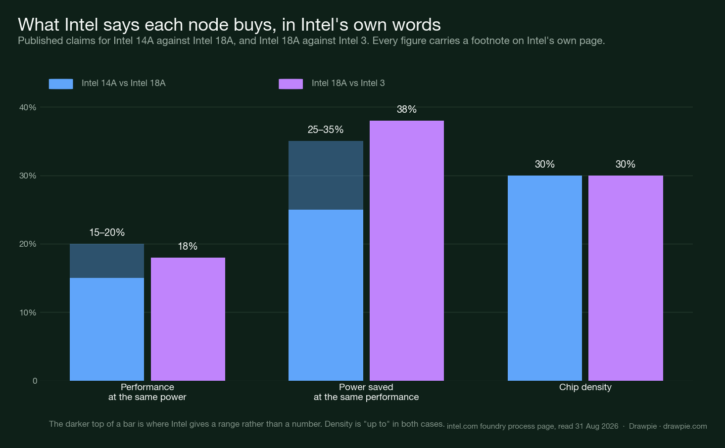
- Intel does publish numbers when it wants to: 14A is claimed at 15–20% more performance at the same power, 25–35% less power at the same performance and up to 30% more density than 18A, each with its own footnote.
- The timeline is the firmest part. Risk production in the second half of 2027 is for Intel’s own products, and the 2028 high-volume ramp was pulled in by a year during the second quarter of 2026.
- Intel Foundry has lost $28.1 billion in operating terms across the last ten reported quarters. The most recent quarter is the series’ highest revenue and smallest loss, and Intel’s own risk disclosure says 14A depends on winning external design commitments.
Intel’s chief financial officer told an investor conference last week that 14A, the company’s next leading-edge process, is shedding defects faster than Intel expected — faster than any node since 22nm. It is a genuinely encouraging thing to say two years before a node ships.
It is also, as stated, impossible for anyone outside Intel to check.
What did Intel actually say about 14A defect density?
That 14A is beating an internal target, and that its rate of improvement is the best Intel has seen since 22nm. David Zinsner, Intel’s CFO, said it at Deutsche Bank’s 2026 Technology Conference on 26 August, an appearance Intel had announced in its own press release eight days earlier.
The two sentences that matter:
“When you look at the defect density, 14A is tracking better than the target curve we had for 14A.”
“It is also doing better than any of the previous nodes in terms of how quickly we are bringing down the defects. In fact, we have not seen this performance since 22nm, which is arguably one of the best nodes Intel has ever put out.”
He said something else in the same conversation that is arguably more informative, and got less attention. Intel’s internal product teams — “probably the most cynical bunch out of anybody”, in his words — have started designing products on 14A. And of the external ones: “They are moving away from just looking at data to thinking about ‘how much capacity can I get?’ ‘what does that supply look like?’”
Why can nobody check this?
Because both halves of the comparison are private. A defect density is a number: defects per square centimetre of wafer, usually written D0. A target curve is a plan for how that number should fall over the months before a node ramps. Intel has published neither.
“Tracking better than the target curve” is therefore a ratio of two unpublished quantities. It could describe a node that is comfortably ahead of an ambitious plan or one that is barely ahead of a soft one, and nothing in the public record distinguishes those.
This is not a company that never gives numbers. Intel’s own process page states that 14A delivers 15–20% more performance at the same power, 25–35% less power at the same performance and up to 30% more density than 18A, each figure carrying its own footnote. The selectivity is the point: the specifications that sell a node are published, and the number that would let you audit its manufacturability is not.
What would make the claim checkable is not complicated, and Intel has done it before. On 4 September 2024, on its own newsroom, Intel’s vice president of technology development wrote that “current Intel 18A defect density” was “already at D0 <0.40” — a number, attached to a node, used to justify cancelling 20A. That is the shape of disclosure 14A has not had. The rest of what would settle it is the same figure for 22nm at the equivalent point in its development, and a note on what counts as a defect in each case.
What would a defect-density number actually tell you?
How much of each wafer survives. Defect density and die area set the yield together, and across the range of densities the industry discusses, a large accelerator lands anywhere from twenty to fifty points below a phone-sized chip cut from the same wafers.
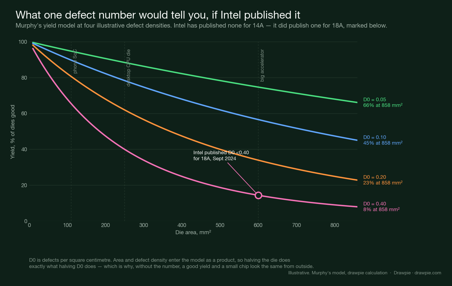
The standard tool is Murphy’s model, which turns a defect density and a die area into an expected yield. The four curves above are illustrative — Intel has published no defect density for 14A, so nobody can draw its curve. The single marked point on the lowest one is not: that is Intel’s own published 18A figure, sitting where it sits. What carries the argument is the shape, and the shape does not depend on the company.
Read across any one of them. At a defect density of 0.10 per square centimetre, a phone-sized die of about 110 mm² yields 90%; a 600 mm² accelerator on the same wafers, with the same defects, yields 57%. The defects have not changed. The chip got bigger, and a bigger chip is a bigger target.
That is why the withheld number is the interesting one. Intel sells these nodes as “optimized for AI, HPC, and next-generation compute”, and that silicon has the largest dies anyone makes. A defect density that is perfectly comfortable for a laptop processor can make a large accelerator uneconomic on the same node. Without the figure, “defects are coming down nicely” and “we can build a 600 mm² part on this” are not the same statement, and only the first has been made.
One more caution, and it is Intel’s own framing that invites it: defect density is not yield. Yield also depends on design rules, on how much redundancy the design carries, on parametric losses that have nothing to do with particles. A good D0 is necessary and not sufficient.
Is “best since 22nm” a big claim?
It is two claims bundled together — one about how fast defects are falling, one about a node Intel ramped in 2012 — and the first is doing most of the work.
The first is about the rate of decline, not the level — Zinsner’s words are “how quickly we are bringing down the defects”. A node can improve rapidly and still be improving from a worse starting point. Nothing in the statement says where 14A’s defect density is, only how fast it is moving.
The second is a comparison to a node from the turn of 2011 into 2012, when Intel put its 22nm Ivy Bridge processors into mass production. It was the company’s first FinFET process, two years ahead of anyone else’s, and by most accounts a very good one. But comparing a defect count measured in 2026 with one measured sixteen years earlier runs into a real problem: inspection tooling has improved enormously in between, and a machine that finds more defects reports a higher defect density on identical wafers. Whether the two numbers are counting the same thing is not something Intel addressed.
And read the sentence for what else it says. If 14A is the best since 22nm, then by Intel’s own measure every node the company brought up in between was worse than this one. That is a plausible reading of Intel’s last decade — it is just an unusual thing to volunteer as good news.
What is 14A supposed to deliver?
15–20% more performance at the same power, 25–35% less power at the same performance, and up to 30% more density than 18A. These are the numbers Intel does publish, each with its own footnote.
14A uses second-generation RibbonFET gate-all-around transistors and PowerDirect, a direct-contact backside power delivery scheme that follows the PowerVia design in 18A. It adds Turbo Cells, which Intel’s own page describes as accelerating CPU and GPU performance “while enabling designers to fine tune block level power performance trade offs for target applications”.
The comparison bar tells its own story. Against Intel 3, the 18A generation claimed up to 18% more performance and 38% less power. Against 18A, 14A claims 15–20% and 25–35%. These are ranges where the previous generation quoted single figures, which is what a node still two years out looks like when a company is being careful.
When does 14A actually arrive?
Risk production in the second half of 2027 for Intel’s own products, and a high-volume ramp in 2028 — a year earlier than Intel used to say.
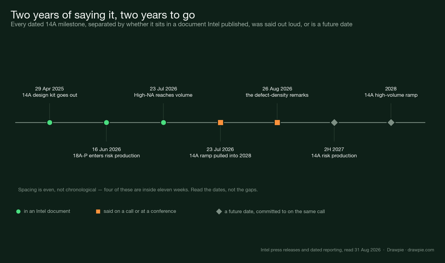
That commitment came from CEO Lip-Bu Tan on the second-quarter earnings call in July: “we remain on track for 14A risk production for our internal products in the second half of 2027, and we made the decision in Q2 to fully commit to high volume ramp in 2028.”
Two details in that sentence repay attention. Risk production is for internal products — external customers are not in that milestone. And the ramp was pulled forward, which is a decision about commitment rather than a report of progress.
Around it, the milestones that do sit in Intel documents: an early 14A process design kit went to lead customers in April 2025, with several saying they intended to build test chips; 18A-P entered risk production in June 2026; and in July Intel said a subset of Panther Lake processors had reached high-volume manufacturing using ASML’s EXE High-NA EUV tools. That last one is the closest thing to a 14A data point in the set, and it needs stating carefully: no Intel document we found says 14A runs on High-NA. What the reporting says is that 14A “will be able to use” it, given the patterning involved. So the fact worth taking is narrower than the headlines — Intel is running High-NA in volume production today, on the generation before.
Why does any of this matter to Intel?
Because the foundry has lost more than two billion dollars in every one of the last ten quarters, and 14A is what it is losing that money for.
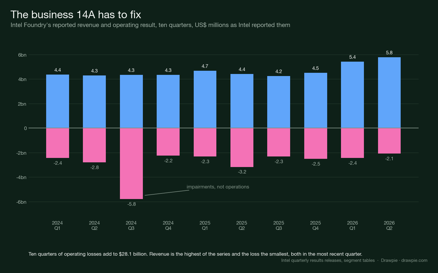
Across the ten quarters Intel has reported since the start of 2024, Intel Foundry’s operating losses add to $28.1 billion. The trend inside that is better than the total suggests: the most recent quarter, ended 27 June 2026, is the highest revenue of the series at $5.77 billion and the smallest operating loss at $2.09 billion, against $3.17 billion a year earlier.
Intel’s own risk disclosure, in the same results release, names what the whole programme turns on — “our pursuit of Intel 14A and other next-generation leading-edge process technologies … and our efforts to secure product design wins with and demand commitments from potential significant external customers”.
Set that beside the CFO’s remarks and the emphasis shifts. The load-bearing sentence was not the one about defects. It was the one about external customers moving away from just looking at data to asking how much capacity they can get — because that is the thing Intel has told regulators the node depends on, and it is the thing a defect-density curve cannot substitute for.
The bottom line
What Intel said is encouraging and, on its face, ordinary corporate optimism of the better kind: a specific technical claim, made by a named executive, at a scheduled public event, two years ahead of a ramp the company has already pulled forward.
What Intel did not say is the number. Until there is a defect density attached to a date, “better than the target curve” is a company grading its own homework and declining to show the paper. The right response is neither to dismiss it nor to treat it as a result — it is to note precisely which sentence would have to be published for it to become one.
Sources
| Source | What it supports here |
|---|---|
| Intel: 14A defect density remarks, reported | All three Zinsner quotations, the caveats about defect counting across sixteen years, and the 22nm background — Ivy Bridge’s mass production at the turn of 2011–12 and the rest of the industry reaching FinFET only in 2014–15 |
| Intel: notice of the Deutsche Bank appearance | That Intel announced the fireside chat, its speakers and the 26 August time and date |
| Intel: investor calendar | The event listing at 10:35 a.m. PDT on 26 August 2026, and that no future events are currently scheduled |
| Intel: foundry process technologies | Every performance, power and density claim for 14A and 18A, RibbonFET 2, PowerDirect and Turbo Cells |
| Intel Foundry Direct Connect, April 2025 | The 14A process design kit going to lead customers, and customers intending to build test chips |
| Intel Foundry at the VLSI Symposium, June 2026 | Intel 18A-P entering risk production on the timeline shared a year earlier |
| Intel: second-quarter 2026 results | The segment table for the latest quarter, Panther Lake in high-volume manufacturing on High-NA EUV, and the 14A risk language |
| Intel: quarterly results releases, 2025–2026 | The ten quarters of Intel Foundry revenue and operating result |
| Intel commits to a 2028 14A ramp, reported | Lip-Bu Tan’s quotation on risk production in the second half of 2027 and the high-volume ramp in 2028 |
| Intel: continued momentum for Intel 18A | The published “D0 <0.40” figure for 18A, its author and its 4 September 2024 date |
Intel pages and reporting read on 31 August 2026. Segment figures are Intel’s own, parsed from the releases linked above. No affiliate links, and no payment was received for any link on this page.
This page describes what Intel has said and reported. It contains no forecast of Intel’s share price, no analyst estimate and no view on the stock, and the yield curves shown are an illustration of a model rather than a measurement of any Intel process.
How we verified this
🔴 No share price, price target, rating or forecast appears anywhere on this page. Intel is a traded company and this site does not publish predictions about traded securities, its own or anyone else’s. What is here instead is what Intel has said about its own operations and what it has already reported — company statements and segment results, which are a different category from a view on the stock.
🔴 The central claim of this article is an absence, so it was checked as one — and then checked again against Intel’s own precedent. Intel’s process page carries the 14A performance, power and density figures and contains the words “defect”, “D0” and “yield” zero times. The Direct Connect release, the VLSI release and the second-quarter results each contain “defect” once, in boilerplate risk language, and “defect density” not at all. Against that, Intel’s newsroom published “D0 <0.40” for 18A on 4 September 2024 over a named executive’s byline. So the claim is not that Intel never publishes this number; it is that Intel published it for the last node and has not for this one.
⚠️ The setting is sourced to Intel and the words are sourced to the reporting, which are different grades of evidence. Two Intel-published documents fix when and where this was said — a notice issued eight days beforehand and the investor calendar entry, which agree on the time to the minute. Neither carries the sentences themselves; Intel said a webcast replay would be available but no transcript could be opened, so the quotations are attributed in the text to the outlet that carried them.
⚠️ The 2027 and 2028 dates are the CEO speaking on an earnings call, not a line in a filing. Lip-Bu Tan’s sentence committing to a 2028 high-volume ramp was said on the second-quarter call of 23 July 2026 and is quoted here from the reporting that carries it verbatim. It is not in Intel’s own results release, which was checked. The timeline chart marks which milestones sit in an Intel document and which were said out loud, because the distinction is the article’s subject.
🔴 The yield curves are illustrative, with one exception that is marked as one. They are Murphy’s model at four round defect densities chosen to span the range the industry discusses, and none of them is a figure Intel has given for 14A. The 0.40 curve does carry a marked point: that is the “D0 <0.40” Intel published for 18A in September 2024, labelled on the chart with the node and the date so it cannot be read as 14A’s. Drawing a yield curve beside an article about a specific company invites exactly the misreading the article is about, so the disclaimer lives in the chart’s own subtitle rather than in the caption.
⚠️ That entry used to say “none of them is Intel’s”, which stopped being true when the 18A figure was added to the chart. It is corrected here rather than quietly rewritten, because a verification note that has drifted from what it describes is worse than none — it certifies the wrong thing with the site’s own voice.
✅ The Intel Foundry figures are parsed out of Intel’s own releases rather than typed. scripts/build_intel_foundry_segment.py reads the supplemental segment table from six quarterly releases, locates the Intel Foundry column by its header rather than by position — Intel renamed its client segment from CCG to CCPG inside this window, so a fixed column index would silently have started reading a different business — and checks that revenue minus costs equals the operating income printed underneath. Quarters that appear in two releases must match exactly, and four of them do.
⚠️ One quarter in that chart is not an operating story and is marked on the chart. The 2024 third-quarter loss of $5.8 billion is several times its neighbours because of impairment charges rather than the cost of running fabs. It is left in because removing an inconvenient quarter is worse, and annotated so it is not read as a trend.
🔴 intel.com refuses both of our usual fetch routes, so the process specifications were read in a browser. Plain requests and the summarising fetcher both return HTTP 403 on intel.com — including for pages that exist, so the status code proves nothing there. The page was opened in a real browser instead. The control: an invented sibling path resolves to a different Intel page with a different title and no 14A section at all, so the reading is of the page we meant.
⚠️ The High-NA connection to 14A is the reporting’s, not Intel’s, and the text now says which. Intel’s own documents put High-NA in high-volume manufacturing for Panther Lake, which is an 18A-family part. None of the Intel pages read here says 14A runs on High-NA; the trade coverage says 14A “will be able to use” it. An earlier draft of this page wrote that High-NA is what 14A leans on, which is a stronger claim than any source supports, and it has been narrowed.
⚠️ No perishes date is set on this page because Intel has not published one to copy. Its investor calendar currently reads “There are no upcoming events scheduled at this time”, so there is no scheduled release date for the next quarterly figures to point at. Every number here is stamped with the quarter or document it came from instead.